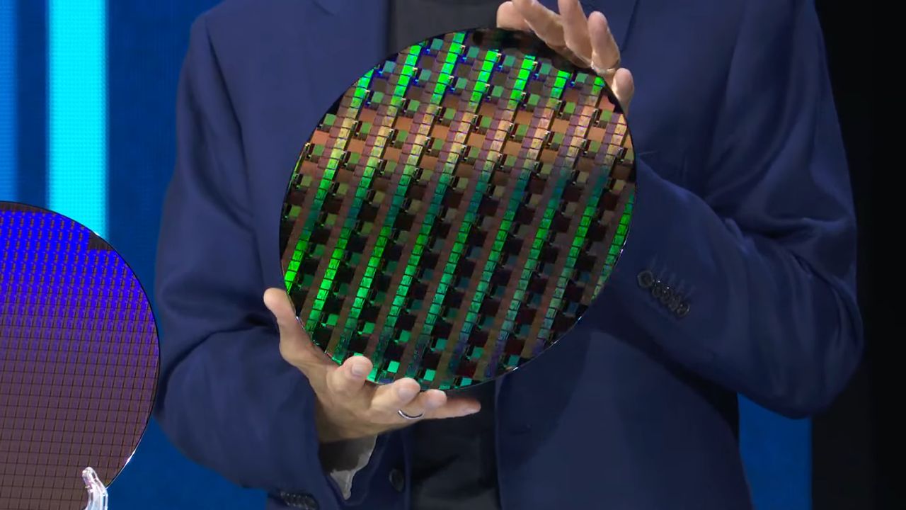
Intel is ramping up production of its CPUs on its 18A (1.8nm-class) process technology with promising results, but at the same time, the work on its enhanced version called 18A-P is well underway with production readiness looming in the coming quarters. The company's 18A-P introduces two new types of transistors, tighter process variability control, and improved thermals to enable higher performance and lower power consumption. This is perhaps why Apple and other fabless chip designers are rumored to be considering using 18A-P.
When compared to Intel's baseline 18A, 18A-P fabrication process promises to enable chip developers to either increase the performance of their designs by 9% (at the same power) or lower their power consumption by 18% (at the same performance and complexity), according to a paper Intel released at the VLSI 2026 conference. To achieve these improvements, Intel introduced new types of gate-all-around RibbonFET transistors, including high-performance devices with enhanced contacts as well as new low-power devices. Designers can now push higher frequencies on critical paths and reduce power consumption in less demanding regions, which greatly improves overall performance efficiency.
Meanwhile, 18A-P retains contacted poly pitch (50nm) and library heights (180nm and 160nm) of 18A as well as design compatibility with the base process, meaning that a chip originally designed for 18A can be ported to 18A-P and benefit from certain process-level improvements (which do not rely on new transistor types), though to fully realize performance and efficiency gains requires design re-optimization.
Article continues below
Another major improvement of 18A-P over 18A is -30% skew corner tightening, which also reduces variability and improves yield efficiency. The enhancement narrows the spread between fast and slow silicon and makes it closer to 'typical' silicon as well as center-to-edge variation across the wafer. Also, the production node adds extra threshold voltage (VT) options (over 5+ pairs of logic VTs compared to 4 pairs in 18A) to enable finer-grained binning and more consistent chip behavior, which increases the proportion of dies that meet target specifications. This improves parametric yield and enables chip designers to get more higher-end silicon from a single wafer. Meanwhile, tightening of process corners does not affect defect density as existing challenges with line-edge roughness (LER) and stochastic variability remain intact.
While Intel's 18A-P retains the contacted pitch of the base node, the company still tweaked the resistance and capacitance of its metal stack, which impacts signal speed, power consumption, and timing. Yet, Intel does not characterize the changes.
Last but not least, 18A-P introduces enhancements in thermals, reliability, and voltage behavior that are critical for an advanced process technology aimed at both client and data center applications. Intel says it improved thermal conductivity by 50%. Lower thermal resistance helps manage higher power densities associated with GAA transistors, which is important for client applications. Improved logic negative-bias temperature instability (NBTI) enhances long-term device stability under high-voltage stress, which is critical for data center processors. Finally, 18A-P better aligns logic and SRAM minimum operating voltage (Vmin) to improve low-voltage operation and stability.
Intel's 18A-P is a heavily optimized version of 18A-P that not only promises higher performance efficiency but also addresses things like parametric yields, thermals, and reliability. Altogether, these enhancements make 18A-P a more mature and attractive version of 18A, not only for Intel, but also for potential external customers like Apple.
Follow Tom's Hardware on Google News, or add us as a preferred source, to get our latest news, analysis, & reviews in your feeds.